address
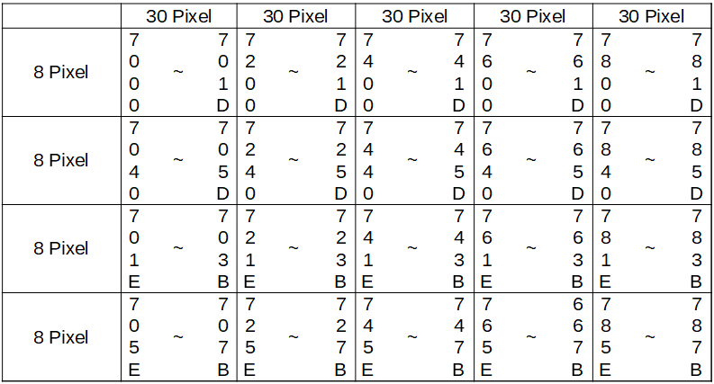
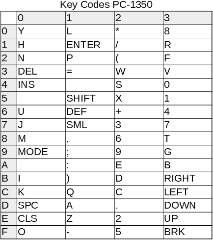
PC-1350 |
address
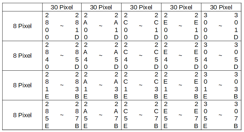
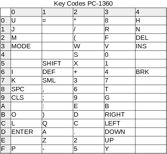
PC-1360 |
description |
| 0436 | 00B5 | keyboard input (PC-1360: identicle to 1E9C); see 46C0 ROM-bank 0 |
| 11B0 | 088A | FAC 1 = (18/19); range 0 to 65535 (*01)(*01a) |
| 11B7 | 0891 | FAC 1 = (18/19); range -32768 to 32767 (*01)(*01a) |
| 162B | 090E | (18) = FAC 1; range 0 to 255 (*01)(*01a) |
| 162F | 0912 | (18/19) = FAC 1; range -32768 to 32767 (*01)(*01a) |
| 163A | 091D | (18/19) = FAC 1; range 0 to 65535 (*01)(*01a) |
| 01AD | 0A74 | FAC 1 = FAC 2 incl. sign in (31) (*01)(*01a) |
| 01B6 | 0A7D | FAC 1 = FAC 2 (*01)(*01b) |
| 01D5 | 0A82 | FAC 1 = FAC 3 incl. sign in (31) (*01)(*01a) |
| 01DE | 0A8B | FAC 1 = FAC 3 (*01)(*01b) |
| 01BB | 0A90 | FAC 1 = FAC 4 incl. sign in (31) (*01)(*01a) |
| 01C4 | 0A99 | FAC 1 = FAC 4 (*01)(*01b) |
| 01C9 | 0AA0 | FAC 2 = FAC 1 incl. sign in (31) (*01)(*01a) |
| 01D2 | 0AA9 | FAC 2 = FAC 1 (*01)(*01b) |
| 019F | 0AAE | FAC 2 = FAC 4 incl. sign in (31) (*01)(*01a) |
| 01A8 | 0AB7 | FAC 2 = FAC 4 (*01)(*01b) |
| 01E6 | 0ABA | FAC 3 = FAC 1 incl. sign in (31) (*01)(*01a) |
| 01EF | 0AC3 | FAC 3 = FAC 1 (*01)(*01b) |
| 01F2 | 0AC6 | FAC 4 = FAC 1 incl. sign in (31) (*01)(*01a) |
| 01FB | 0ACF | FAC 4 = FAC 1 (*01)(*01b) |
| 0193 | 0AD2 | FAC 4 = FAC 2 incl. sign in (31) (*01)(*01a) |
| 019C | 0ADB | FAC 4 = FAC 2 (*01)(*01b) |
| 01E3 | 0ADE | FAC 3 = FAC 2 (*01)(*01b) |
| 0202 | 0B8A | FAC 1 <-> FAC 2 incl. sign in (31) (*01)(*01a) |
| 020F | 0B97 | FAC 1 <-> FAC 2 (*01)(*01b) |
| 013F | 0BDB | FAC 1 = 0; (31) incl. sign in (31) (*01)(*01a) |
| 0142 | 0BDE | FAC 1 = 0 (*01)(*01b) |
| 0133 | 0BE5 | FAC 2 = 0; (31) incl. sign in (31) (*01)(*01a) |
| 0139 | 0BEB | FAC 3 = 0; (31) incl. sign in (31) (*01)(*01a) |
| 0166 | 0BF1 | Mantissa from FAC 1 = 0; sign and exp. are not changed (*01) |
| 0160 | 0BFB | Mantissa from FAC 2 = 0; sign and exp. are not changed (*01) |
| 0163 | 0BFE | Mantissa from FAC 4 = 0; sign and exp. are not changed (*01) |
| 017D | 0C01 | sign and exp. from FAC 1 = 0 (*01)(*01b) |
| 017A | 0C08 | sign and exp. from FAC 2 = 0 (*01)(*01b) |
| 0153 | 0C0B | FAC 2 = 1 incl. sign in (31) (*01)(*01a) |
| 06B9 | 0C18 | FAC 2 = 0.6 incl. sign in (31) (*01)(*01a) |
| 0732 | 0C24 | constants for type of angle conversion: |
| | DEG: FAC 2 = 0.434294481903 incl. sign in (31) (*01)(*01a) |
| | GRAD: FAC 2 = 0.9 incl. sign in (31) (*01)(*01a) |
| | RAD: FAC 2 = 57.2957795131 incl. sign in (31) (*01)(*01a) |
| 0BEC | 0C54 | FAC 2 = PI = 3.141592653 incl. sign in (31) (*01)(*01a) |
| 0301 | 0D42 | (31)=sign FAC 1 and FAC 2; (FE71)=SP+2 (PC-1350: (6F3F)=SP+2); (30)=00 (*01)(*01b) |
| 0310 | 0D64 | (31)=sign FAC 1; (FE71)=SP+2 (PC-1350: (6F3F)=SP+2); (30)=00 (*01)(*01b) |
| 0328 | 0D69 | sign from (31) -> FAC 1 and FAC 2 (*01)(*01b) |
| 0333 | 0D74 | sign from (31) -> FAC 1 (*01)(*01b) |
| 10E4 | 10B9 | ERROR 2 (*03) |
| 10EC | 10C0 | ERROR 1 (*03) |
| 10F0 | 10C8 | ERROR 3 (*03) |
| 10F4 | 10CD | ERROR 4 (*03) |
| 10F8 | 10D2 | ERROR 5 (*03) |
| 10FC | 10D7 | ERROR 6 (*03) |
| 10E6 | 10BB | ERROR A (1 <= A <= 9) |
| 1100 | 10DC | ERROR 7 (*03) |
| 1104 | 10E1 | ERROR 8 (*03) |
| 1108 | 10E6 | ERROR 9 (*03) |
| 027D | 1108 | D = AE |
| 0282 | 110D | S = AE |
| 0287 | 1112 | S = AE+1 |
| 028D | 1118 | D = AE+1 |
| 0297 | 111E | S = AE-1 |
| 02B5 | 1124 | D = AE-1 |
| 1414 | 112A | D = S |
| 1419 | 112F | S = D |
| 1553 | 1134 | (0C/0D) = S |
| 1558 | 1139 | (0C/0D) = D |
| 113E | D <-> (0C/0D) |
| 161A | 1143 | S <-> (0C/0D) |
| 170E | 1148 | A = (0A); (0A) = (06) |
| 1713 | 114D | (0B) = (06); A = (06) |
| 115C | 1153 | push S |
| 1167 | 115E | pop S |
| 141E | 1188 | (38/39) = S |
| 140B | 1192 | S = (38/39) |
| 108E | 1197 | S <-> (38/39) |
| 119C | S <-> D |
| 11A6 | 11A1 | S = (1D/1E)-1 == STR 2 (*01) |
| 11AA | 11A5 | S = (15/16)-1 == STR 1 (*01) |
98B0 v0
9A36 v1 | 11AB | AE = (FFDB/DC) (PC:1350: 6F05/06) start of last MERGE-block |
98B6 v0
9A3C v1 | 11B1 | AE = (FFD9/DA) (PC:1350: 6F03/04) end of basic memory |
| 0293 | 11B7 | S = FD1F (PC-1350: 6EAF) Inputbuffer (ASCII or token) |
| 11BB | S = AE-1 |
| 029D | 11C1 | S = FBFF (PC-1350: 767F) operand-stack |
| 02A3 | 11C7 | S = FD7F (PC-1350: 6CFF) displaybuffer |
| 02AA | 11CE | D = FD7F (PC-1350: 6CFF) displaybuffer |
| 02B1 | 11D5 | D = FD1F (PC-1350: 6EAF) inputbuffer |
| 02BB | 11DF | D = FBFF (PC-1350: 767F) operand-stack |
| 11E5 | S = (FEF0/F1) start basic programm |
| 1471 | 11EB | S = (FFD7/D8) (PC-1350: 6F01/02) start basic memory |
| 11F1 | (FFDB/DC) = (FFD7/D8) using AE |
| 11FC | (FEF0/F1) = (FFDB/DC) using AE |
| 1207 | (FEF0/F1) = (FFD7/D8) using (0A/0B) |
| 1D84 | 1212 | (2AB4/B5) = S (PC-1350: (6F20/21) = S); save S for analyse basic program (*03) |
| 1D89 | 1217 | S = (2AB4/B5) (PC-1350: S = (6F20/21)); S = restore address at end of basic-command (*03) |
| 1175 | 1233 | E mal (+D) = (+S) |
| 1265 | FDE8..EF = 00 temp memory for FAC 1 (*01) |
| 126E | FAC 4 = FAC 1 (*01)(*01b) |
| 1275 | FAC 1 = FAC 4 (*01)(*01b) |
| 127C | FAC 2 = FAC 1 (*01)(*01b) |
| 1283 | Call 40(MM) in rom bank Q (lo nibble) and returns to rom bank Q (hi nibble) |
| 12DB | A = (+S) from both RAM bank (*02) |
| 12FC | A = (-S) from both RAM bank (*02) |
| 131B | (+D) = A to both RAM bank (*02) |
| 133C | (-D) = A to both RAM bank (*02) |
| 142B | 13A3 | activate RAM bank 0 |
| 1438 | 13A9 | activate RAM bank 1 |
| 13AF | wait A * 2 ms |
| 09E8 | 13B7 | wait 6 ms |
| 04AD | 13C4 | CR = 00; display off |
| 04B1 | 13C8 | CR = 01; display on |
| 1441 | FAC 1 = 00; FAC 2 = 00; FAC 3 = 00 (*01)(*01b) |
| 1C44 | 1448 | FD80..AF = 20 (PC-1350: 6D00..6D2F); clear 1.+2. line of displaybuffer |
| 1C3F | 144D | FD98..AF = 20 (PC-1350: 6D18..6D2F); clear 2nd line of displaybuffer |
| 1C36 | 1452 | FD80..97 = 20 (PC-1350: 6D00..6D17); clear 1st line of displaybuffer |
| 1D3B | 1483 | (10)..(27) <-> FDC8..DF (PC-1350: 6D48..5F); 4th line .Zeileof displaybuffer |
| 1D43 | 148B | (10)..(27) <-> FD80..97 (PC-1350: 6D00..17); 1st line of displaybuffer |
| 1D48 | 1490 | (10)..(27) <-> FD98..AF (PC-1350: 6D18..2F); 2nd line of displaybuffer |
| 1D4D | 1495 | (10)..(27) <-> FDB0..C7 (PC-1350: 6D30..47); 3rd line of displaybuffer |
| 1E0C | 14B6 | FD80..DF = 20 (PC-1350: 6D00..5F); clear displaybuffer (24x4) |
| 14BF | FD80..A3 = 20 (PC-1350: 6D00..23); clear displaybuffer (18x2) |
| 1C1C | 14C8 | FD20..6F = 0D (PC-1350: 6EB0..FF); clear input-buffer |
| 1517 | BIT(FF30),80; SIO open |
| 15C5 | 2A98..AF = 00; printer-buffer CE-126P |
| 1CD0 | 16B5 | D = address display memory -1 for line A 2800/2840/281E/285E (PC-1350: 7000/7040/701E/705E) |
| 1CEF | 16D4 | D = address display memory-1 for cursor X=(FD10)/Y=(FD11) (PC-1350: X=7881/Y=7880) |
| 1D5A | 1710 | D = address displaybuffer according line for cursor Y=(FD11) (PC-1350: 7880) |
| 1D70 | 1726 | D = FD80 (PC-1350: 6D00); 1st line displaybuffer |
| 1D74 | 1731 | D = FD98 (PC-1350: 6D18); 2nd line displaybuffer |
| 1735 | D = FD92; 2nd line displaybuffer (18x2) |
| 1D78 | 1739 | D = FDB0 (PC-1350: 6D30); 3rd line displaybuffer |
| 1D7C | 173D | D = FDC8 (PC-1350: 6D48); 4th line displaybuffer |
| 15EC | 17C4 | FEE0..E3 = 00 (PC-1350: 6F39..3C); clear USING-format |
| 1410 | 18A3 | CMP (14),D0; test FAC 1 for string |
| 8081 | 18AD | A = '<' or '>', depending on bit 6 from (&FFEC; PC-1350: &6F16); TEXT-mode |
| 10C1 | 18D9 | FAC 1 = (POP value operand-stack (&FC00; PC-1350: &7680)) (*01)(*01b) |
| 10AA | 18DD | FAC 2 = (POP value operand-stack (&FC00; PC-1350: &7680)) (*01)(*01b) |
| 1737 | 19B0 | (+D) = 2D; -"" |
| 19F7 | (P) = 0; (P+1) = 0 |
| 1DF3 | 1A18 | display line, A=0..3, A=4->line 0..3, see ROM bank 1, 4004 |
8962 v0
8AB8 v1 | 1E80 | FAC 1 = FAC 2 + FAC 1 (*01)(*01a) |
8979 v0
8ACF v1 | 1E84 | FAC 1 = FAC 2 - FAC 1 (*01)(*01a) |
8983 v0
8AD9 v1 | 1E88 | FAC 1 = FAC 2 * FAC 1 (*01)(*01a) |
898D v0
8AE3 v1 | 1E8C | FAC 1 = FAC 2 / FAC 1 (*01)(*01a) |
| 04B1 | 1E94 | enable display == JP,13C8 |
| 04AD | 1E98 | disable display == JP,13C4 |
| 0436 | 1E9C | keyboard input (PC-1360: identicle to 1E9C); see 46C0 ROM-bank 0 |
89AC v0
8B02 v1 | 1EC0 | FAC 1 = EXP(FAC 1) (*01)(*01a) |
89BA v0
8B10 v1 | 1EC4 | FAC 1 = SIN(FAC 1) (*01)(*01a) |
89C1 v0
8B17 v1 | 1EC8 | FAC 1 = COS(FAC 1) (*01)(*01a) |
89C8 v0
8B1E v1 | 1ECC | FAC 1 = TAN(FAC 1) (*01)(*01a) |
89CF v0
8B25 v1 | 1ED0 | FAC 1 = ASN(FAC 1) (*01)(*01a) |
89D6 v0
8B2C v1 | 1ED4 | FAC 1 = ACS(FAC 1) (*01)(*01a) |
89DD v0
8B33 v1 | 1ED8 | FAC 1 = ATN(FAC 1) (*01)(*01a) |
89EB v0
8B41 v1 | 1EDC | FAC 1 = DEG(FAC 1) (*01)(*01a) |
89F2 v0
8B48 v1 | 1EE0 | FAC 1 = DMS(FAC 1) (*01)(*01a) |
8E9F v0
8FF4 v1 | 1EE4 | FAC 1 = ABS(FAC 1) (*01)(*01a) |
8E7B v0
8FD0 v1 | 1EE8 | FAC 1 = INT(FAC 1) (*01)(*01a) |
8A00 v0
8B56 v1 | 1EEC | FAC 1 = SGN(FAC 1) (*01)(*01a) |
89F9 v0
8B4F v1 | 1EF0 | FAC 1 = RND(FAC 1) (*01)(*01a) |
89B3 v0
8B09 v1 | 1EF4 | FAC 1 = SQR(FAC 1) (*01)(*01a) |
89A5 v0
8AFB v1 | 1EF8 | FAC 1 = LOG(FAC 1) (*01)(*01a) |
899D v0
8AF3 v1 | 1EFC | FAC 1 = LN(FAC 1) (*01)(*01a) |
8B1E v0
8C74 v1 | 1F00 | FAC 1 = ASC(STR 1) (*01)(*01a) |
8B3E v0
8C94 v1 | 1F04 | STR 1 = CHR$(FAC 1) (*01)(*01a) |
8BA6 v0
8CFC v1 | 1F08 | STR 1 = STR$(FAC 1) (*01)(*01a) |
8C02 v0
8D58 v1 | 1F0C | FAC 1 = VAL(STR 1) (*01)(*01a) |
| 142B | | activate RAM bank 1 |
| 1438 | | activate RAM bank 0 |
| 144D | | (+S) from RAM bank 0 (S < &8000) or bank 1 (S >= &8000) |
| 1454 | | if S >= &8000 then activate RAM bank 1 |
| 153B | | X = 783C (status display) |
| (*01) |
The following internal variables/addresses are used:
| variable | address | number sign |
|---|
| FAC 1 | 10..17 | (31) bit0 = &01 if mantissa is negative |
| FAC 2 | 18..1F | (31) bit1 = &02 if mantissa is negative |
| FAC 3 | 20..27 | (31) bit2 = &04 if mantissa is negative |
| FAC 4 | 28..2F | (31) bit3 = &08 if mantissa is negative |
| STR 1 | 14 = D0 | |
| 15 = address LO | |
| 16 = address HI | |
| 17 = length | |
| STR 2 | 1C..1F | |
FAC 1..4 are in BCD format like it's used for numeric variables
(31) und collon 'number sign': see also (*01a) and (*01b)
Each function meight destroy FAC 1..4 (STR 1..2) during operation. They meight be used for internal calculations.
(The flags (33) and (37) that are used within rou rountes donät have to be set when calling a ROM function. They only are used for internal purpose als temporary flags during calculation).
Some exsamples:
| number | floating point format (BCD) |
| 6 | 00 00 60 00 00 00 00 00 |
| 60 | 00 10 60 00 00 00 00 00 |
| 0.6 | 99 90 60 00 00 00 00 00 |
| 0.06 | 99 80 60 00 00 00 00 00 |
| -0.6 | 99 98 60 00 00 00 00 00 |
| -6 | 00 08 60 00 00 00 00 00 |
nibble 0-2 stands for the exponent:
For positive number: 0 0 0 to 0 9 9 -> number = mantissa*10^0 to 10^99
For negative number: 9 9 9 to 9 0 1 -> number = mantissa*10^-(1000-999) to 10^-(1000-901) (== 10^-1 to 10^-99)
nibble 3-15 are the mantissa:
For positive number: nibble 3 == 0
For negative numbers: Nibble 3 == 8
nibble 4-15 is the mantissa (for leading zeros then exponent is used).
nibble 14-15 only is used internally for rounding purpose but is not displayed.
|
| (*01a) |
The sign of FAC 1..4 must not be set in (31) before calling the function.
Functions marked with (*1a) set (31) internally if needed and also copy it back from (31) to FAC 1..4 after calculation.
|
| (*01b) |
The sign for FAC 1..4 must be copied to (31) and should be deleted in FAC 1..4 before calling the function.
This can be done by calling 0D64/0D42 (PC-1360) or 0310/0301 (PC-1350)
(31) indicates the sign of FAC 1..4 after calling the function and should be written to FAC 1..4
This can be done by calling 0D74/0D69 (PC-1360) or 0333/0328 (PC-1350).
Functions not marked with (*01b) don't set (31) from FAC 1..4 but rely on it for calculation.
|
| (*02) |
If the logical basic memory starts at < &8000 (MEM "B" or MEM "D"):
- address &0000 to &7FFF:
- activate RAM bank 0
- read/write (address + &8000)
- activate RAM bank 1
- address &8000 to &FFFF:
- (address) read/write from/to RAM bank 1
Sonst (MEM "C"):
-
(address) read/write from/to RAM bank 0
|
| (*03) |
PC-1360: 2AB4/B5 , PC-1350: 6F20/21
S is stored at this address after all parameters of a basic command were analysed.
The basic interpreter will continue execution at (S+1).
Example:
The assembler program expects, separated by a comma, a numeric parameter:
The Basic-Programm will be stopped with ERROR 1, if no comma as given after the CALL statement
Example PC-1360 (address: 8100)

100: CALL &8100,G


LD A,(+S)

CMP A,2C

JP Z,+09 ; comma found

; Error 1 (no comma found)

POP A    ; delete return address auf basic command CALL

POP A

DEC S    ; set S to the last read char

JSR 1212 ; 2AB4/B5 = S

JP,10C0  ; end program with ERROR 1

JSR,4016 ; FAC1 = argument starting at (S+1), ROM-bank 0 (in the example value of variable G)

JSR 1212 ; 2AB4/B5 = S

....     ; use FAC1

RET      ; end basic extension (== CALL command)
Example PC-1350 (address: 6100)

100: CALL &6100,G


LD A,(+S)

CMP A,2C

JP Z,+09 ; comma found

; Error 1 (no comma found)

POP A    ; delete return address auf basic command CALL

POP A

DEC S    ; set S to the last read char

JSR 1D84 ; 6F20/21 = S

JP,10EC  ; end program with ERROR 1

JSR,8039 ; FAC1 = argument starting at (S+1) (in the example value of variable G)

JSR 1D84 ; 6F20/21 = S

....     ; use FAC1

RET      ; end basic extension (== CALL command)
|